
Compact laser head
A small head mounts directly on the motion system, close to the optics, so the machine stays compact.

Applications Glass processing
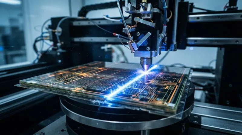
Through-glass vias for advanced packaging, with no microcracks. The femtosecond laser modifies the glass, selective etching opens the via, and the throughput scales with the number of lasers on the line.
[value] µm
Smallest via diameter in 0.5 mm borosilicate glass.
1 : [value]
Aspect ratio after selective etching.
[value] vias/s
Modification rate per laser head.
From problem to process
01 · Problem
Glass interposers and substrates need dense via arrays. Mechanical drilling, CO2 and nanosecond lasers leave microcracks, heat-affected zones and taper that fail in reliability testing.
02 · Requirement
03 · Process
Femtosecond pulses are absorbed only at the focus, inside the glass. They change the material along the via path without cracking it. A wet etch then removes the modified glass far faster than the bulk, opening a clean via.

A small head mounts directly on the motion system, close to the optics, so the machine stays compact.

No chiller and no water lines in the cleanroom. Fewer utilities to plan, fewer parts to service.

CAN and USB control, TTL pulse-picker triggering and an analog power input connect to the machine controller.

Run several lasers side by side over one panel. Throughput grows with each head, not with a bigger laser.
Evidence
Microscope images from LITILIT test runs. Every sample lists its material, thickness and magnification.
[Customer] tested one INDYLIT 20 on glass interposer samples, then moved to [number] lasers on their production line. Here is how the process window and the order grew.
Read the case studyStarting parameters from our lab. Your material, thickness and design will move them, so we confirm every number on your own samples.
The laser we recommend for this process.
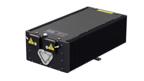
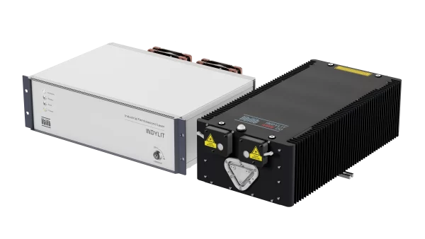
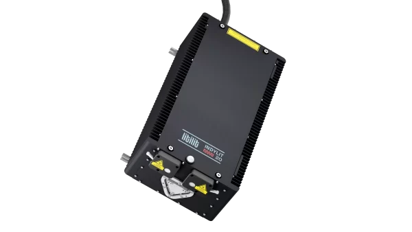
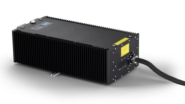
Up to 20 W at 1 MHz, with an optional 515 nm green module, for high-rate processing of glass panels.
 380 fs pulses
 1030 / 515 nm
 Passively air cooled

Ship samples to our Vilnius application lab. We process them to your via design and return the parts with microscope images and the parameters we used.
Tell us the material and the result you need. A laser engineer replies within [response time].
Ask about lead times, volume pricing, supply capacity and long-term availability.
Request a quote