
Compact laser head
Integrates into wafer processing tools where space is limited.

Applications Semiconductor
Dicing, grooving and drilling of thin wafers and brittle materials with minimal chipping and debris. We are building process data with partners and would like to test your application.
[value] µm
Kerf width on [value] µm silicon.
[value] µm
Edge chipping after dicing.
[value] mm/s
Grooving speed on [material].
From problem to process
01 · Problem
As wafers get thinner and dies smaller, blade dicing causes chipping and cracks. Longer-pulse lasers leave heat damage and debris that lower die strength and yield.
02 · Requirement
03 · Process
Femtosecond pulses ablate thin layers of silicon, low-k films and other materials before heat spreads, giving narrow, clean cuts and grooves on fragile wafers.

Integrates into wafer processing tools where space is limited.

No water lines near the wafer and fewer utilities in the fab.

Add lasers to raise throughput without changing the process.

Standard interfaces for tool controllers and automation.
Evidence
Microscope images from LITILIT test runs. Every sample lists its material, thickness and magnification.
We are running a joint process study with [partner] on [material]. Results will be published here once they are confirmed.
Read the case studyStarting parameters from our lab. Your material, thickness and design will move them, so we confirm every number on your own samples.
The laser we recommend for this process.
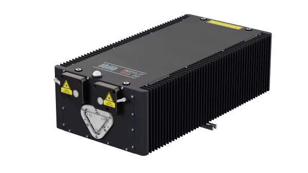
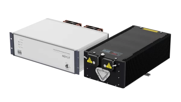
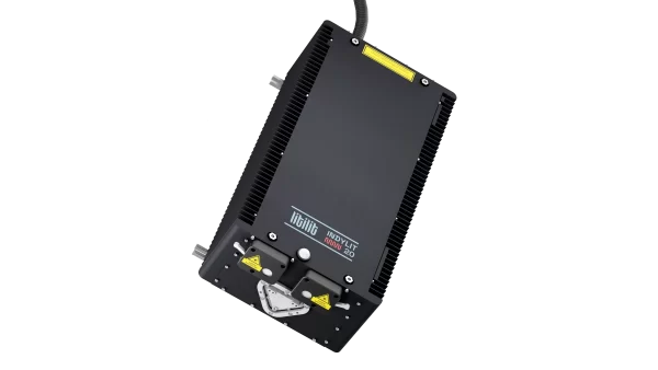
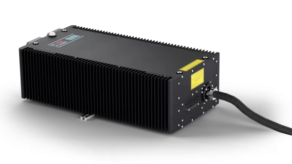
Up to 20 W at 1 MHz, with an optional 515 nm green module, for wafer processing.
 380 fs pulses
 1030 / 515 nm
 Passively air cooled

Send samples to our Vilnius application lab. We process them, share the results and parameters, and plan the next step with your team.
Tell us the material and the result you need. A laser engineer replies within [response time].
Ask about lead times, volume pricing, supply capacity and long-term availability.
Request a quote